FMCW Hardware
1 System Structure
The system consists of C-band FMCW radar RF Front-end and FPGA high-speed acquisition system.
2 FMCW radar RF Front-end performance
C-band FMCW radar RF Front-end main technical performance:
- Sweep bandwidth: 5.2 ~ 8.2 GHz (customizable)
- Sweep time: 1 μs
- Output power: 30 dBm
- Sweep mode: triangle wave sweep
| Parameter | Symbol | Value | Unit | Comment/Test Condition |
|---|---|---|---|---|
| Voltage | Vcc | 220 | V | Three sets of terminal adapters for AIWISE, pay attention to grounding |
| Bandwidth | Freq | 5.2 ~ 8.2 | GHz | customizable |
| Sweep Time | Tsweep | 1 | μs | customizable |
| Harmonic Suppression | HS | >30 | dB | |
| Operating Temperature | $T_a$ | -20 ~ 85 | ℃ | Customizable industrial -40 ℃ |
| Output Power | Pout | 30 | dBm | customizable |
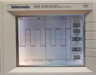
| Sync Pulse | Vsync | 3.3 | V | The trailing edge of the pulse represents the beginning of chirp (eg.figure 4) |
| RF Gain | Gain | 45 | dB | MAX to 60 dB |
2.1 FMCW radar RF Front-end introduction
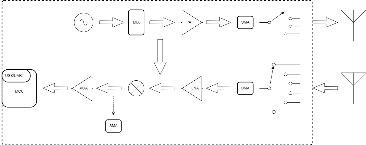
As shown in Figure.1, This is the RF Front-end of C-band FMCW radar, which can cover 5.2 ~ 8.2 GHz. The built-in signal source outputs FMCW signals. The frequency sweep mode is triangular frequency sweep, and THE SMA rf output provides synchronous pulse interface, which is used to prompt the start of each chirp. It can be used in time division MIMO array radar structure.Including rf transmitting chain and receiving chain, the output power of the transmitting is 30 dBm. The gain of the receiving chain is 45 dB, and the GFLNA03 external amplifier can be selected to increase the gain of the receiving chain to more than 60 dB.The RF Front-end adopts active and passive RF devices from professional RF device manufacturers. The RF connectors and circuit boards used have been tested and verified for many times, which meet the requirements of this frequency band without obvious dispersion and multi-mode effect, and can transmit rf signals of this frequency band well.
2.2 FMCW radar RF Front-end appearance
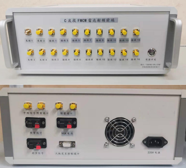
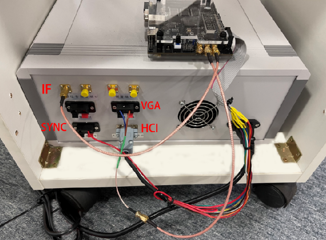
Figure.2 shows the appearance of FMCW radar RF Front-end. The SMA receives or outputs RF signals. On the back, it is equipped with synchronous signal output interface, VGA control voltage interface and intermediate frequency output interface. As a data acquisition board, the FPGA acquisition board can intuitively display the movement of the measured object after being connected to the antenna.
2.3 FMCW radar RF Front-end interface
- The power interface: The power supply is 220V AC
- Synchronous signal output interface: Red is the positive pole and black is the negative pole. The synchronous square wave as shown in Figure.3 is output to prompt the start of chirp.The synchronous pulse interface provides 3.3V pulse, the rising edge of which is the beginning of frequency sweep, and can be used to trigger the switching of transmitting and receiving switches in MIMO array radar structure.
-
VGA voltage interface: Red is the positive pole, black is the negative pole, connected to the experimental power supply, the voltage range of 0 ~ 1V, the larger the voltage, the greater the amplitude of the intermediate frequency signal.
-
Human-computer interaction control interface: The device has a built-in 16-channel receiving switch and a 4-channel transmitting switch. The channel can be switched through the control switch, so that more complex algorithm operation can be carried out, and more information can be obtained. MIMO array radar can be formed through multiple channels, and the chirp synchronization signal switching switch in Figure.3 can also be fully utilized. Control wire terminals are equipped with wires of different colors. Switching on and off of each channel can be controlled according to the color and corresponding level of wires in the table. The black wire shall be connected to the ground wire of the customer's GND.Note:that the high level of the control signal is 3.3V
The truth table of the 16-channel switch at the RX:
RX_SW1_C WHITE RX_SW1_B YELLOW RX_SW1_A BLUE TX_SW1_C PURPLE TX_SW1_B GREEN TX_SW1_A GRAY SW_ST1_VC BROWN Channel 0 0 0 0 0 0 1 RF1 0 0 0 0 0 1 1 RF2 0 0 0 0 1 0 1 RF3 0 0 0 0 1 1 1 RF4 0 0 0 1 0 0 1 RF5 0 0 0 1 0 1 1 RF6 0 0 0 1 1 0 1 RF7 0 0 0 1 1 1 1 RF8 0 0 0 0 0 0 0 RF9 0 0 1 0 0 0 0 RF10 0 1 0 0 0 0 0 RF11 0 1 1 0 0 0 0 RF12 1 0 0 0 0 0 0 RF13 1 0 1 0 0 0 0 RF14 1 1 0 0 0 0 0 RF15 1 1 1 0 0 0 0 RF16 The truth table of the 4-channel switch at the TX:
RED ORANGE Channel 0 0 IN to RF1 1 0 IN to RF2 0 1 IN to RF3 1 1 IN to RF4 - Intermediate frequency signal out interface: IF signal
- Set aside Interface
3 FPGA high-speed acquisition system (AW-UWB-DIG-INT)
FPGA high-speed acquisition system is mainly composed of FPGA data acquisition board and the product model is AW-UWB-DIG-INT.
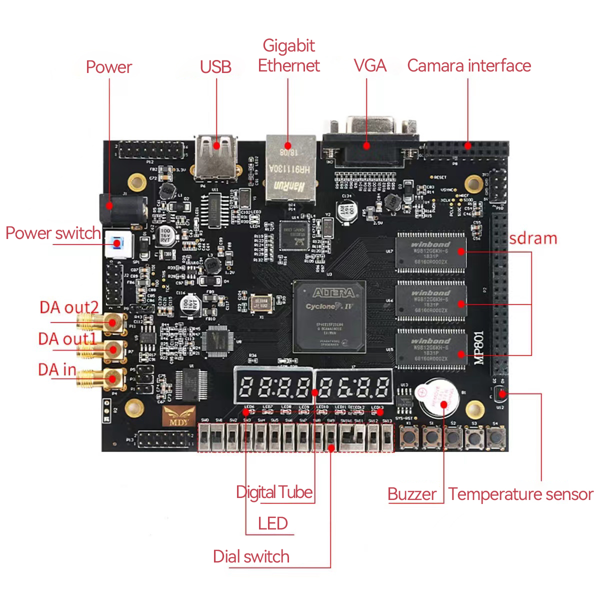
3.1 FPGA data acquisition board introduction
Eg. Figure.4,FPGA data acquisition board is based on Altera Cyclone IV EP4CE15F23C8, with 15K logical resources, 504K bit RAM resources, and three onboard 128M bit SDRAM, which is suitable for storing large-capacity data. Moreover, it has the high-speed parallel DA chip AD9709 with 125Mhz dual-channel conversion rate and the high-speed parallel AD chip AD9280 with 32Mhz conversion rate, and adopts 64M SPI flash memory and is equipped with ultra-high speed gigabit network port, which is rich in resources to meet the needs of secondary development.
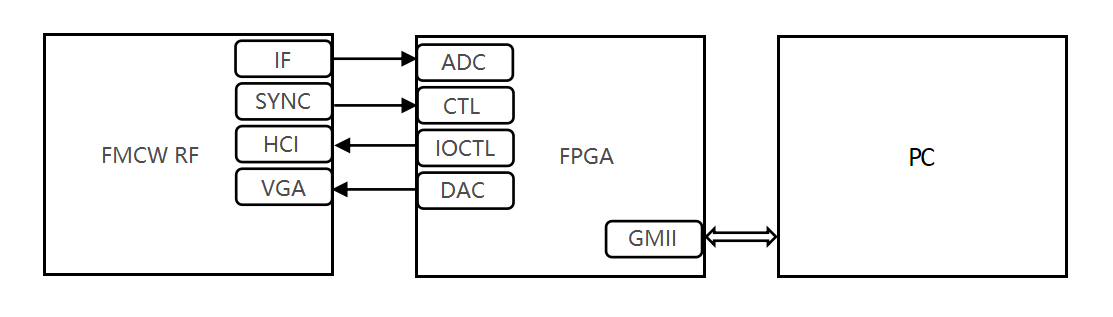
3.2 FPGA system chart
The system chart of the whole system is shown in Figure.5 . The FPGA acquisition board uses ADC to collect AW-UWB-DIG-INT intermediate frequency signal, carries out frame statistics and antenna switching through synchronous signal, and uploads the data to PC through network port, which stores and processes the data. At the same time, the AW-UWB-DIG-INT transmitting and receiving channels can be configured through PC. After being transmitted to FPGA through network port, the AW-UWB-DIG-INT can be configured according to the human-computer interaction configuration table. At the same time, the corresponding voltage can be output by DAC to control VGA gain.
4 Quick start
- First of all, the antenna of AW-UWB-DIG-INT should be properly connected, so that it can not be vacant in case of burning out. 16 transmitting antennas and 4 receiving antennas are connected as required.
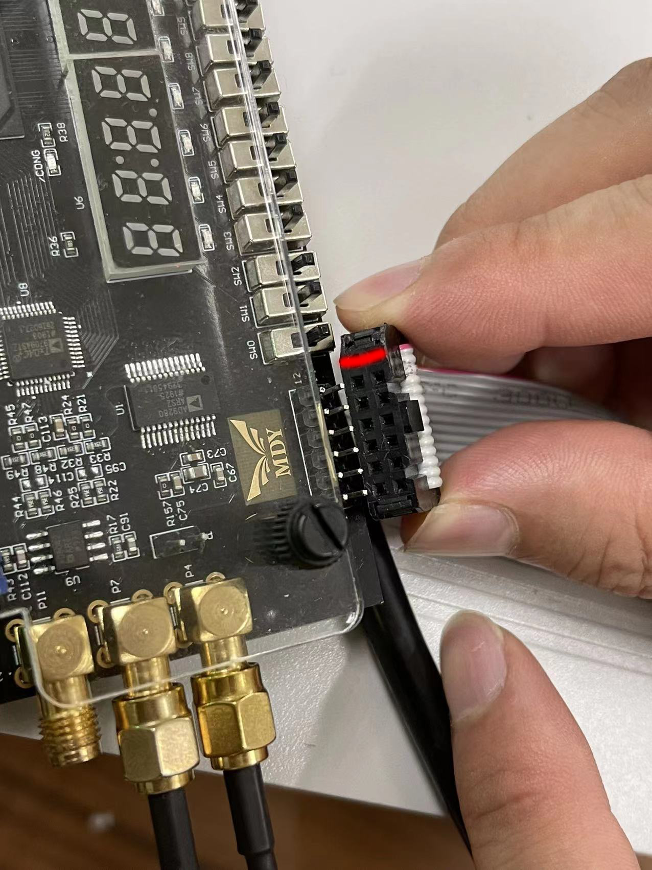
- Connect FPGA to FMWC, as shown in the figure.6.
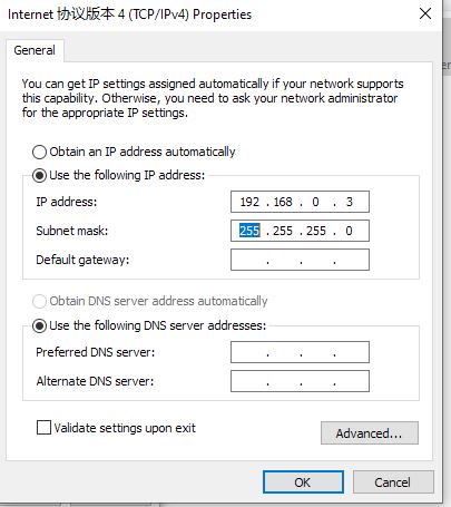
- Connect the FPGA acquisition board to the PC through the USB-to-gigabit network port adapter. After the cable is connected, configure the IP address as shown in the figure.7.
- Power on the FPGA acquisition board and then AW-UWB-DIG-INT.
- After power-on, data is automatically collected and uploaded. Configure relevant antenna channels and process data through PC.